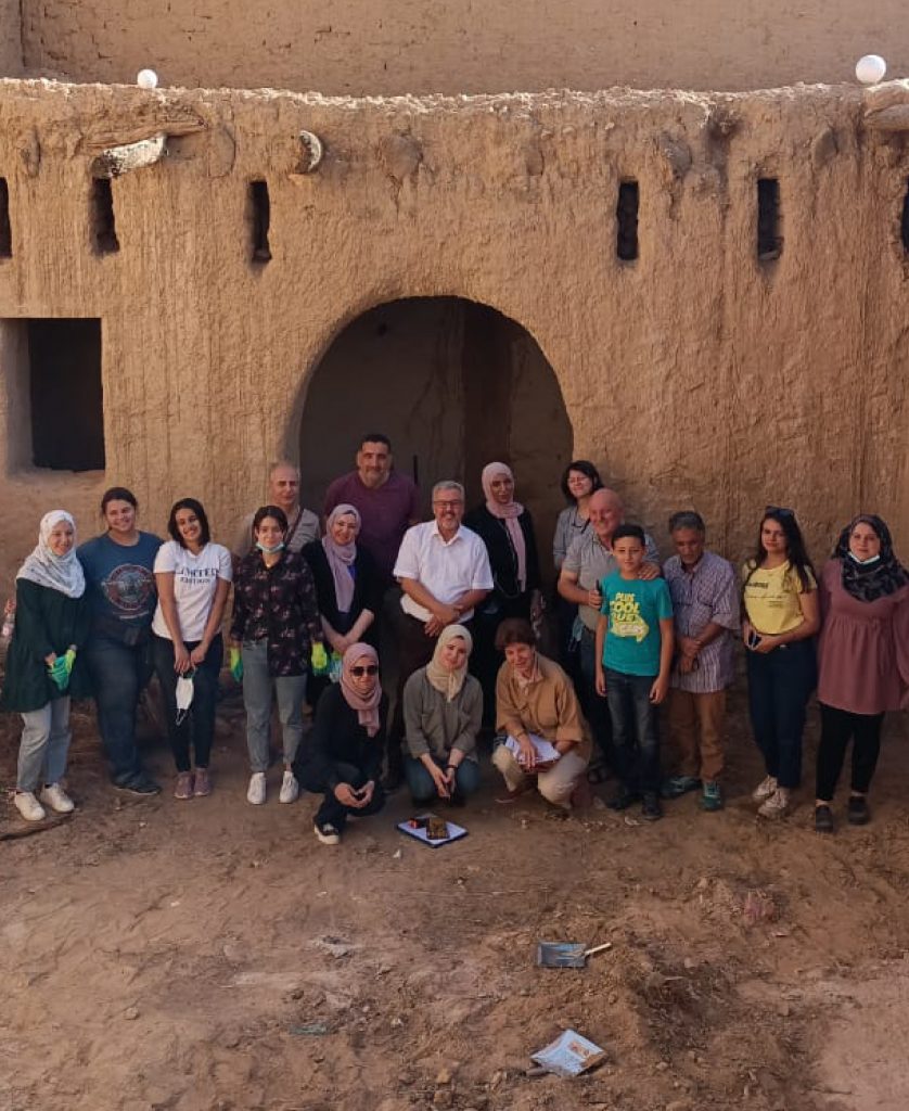
Alumni politecnico di milano
Politecnico di Milano and STMicroelectronics,have inaugurated the expansion of semiconductor manufacturing capabilities at PoliFab, the University’s micro- and nanotechnology R&D center. A laboratory created to provide the highest technological standards for a wide range of applications and processes involving the five Key Enabling Technologies: photonics, micro and nanoelectronics, biotechnologies, advanced materials and nanotechnology.
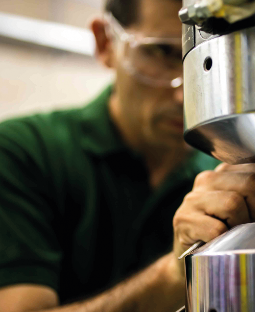
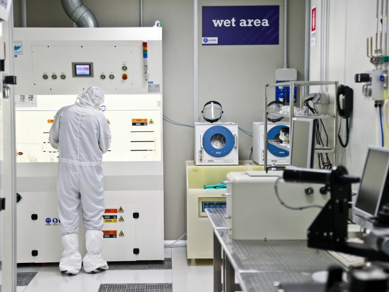
Building on the long-standing collaboration between the two organizations, the PoliFab’s clean room – a facility where silicon wafers are made into semiconductor chips – has received state-of-the-art equipment from STMicroelectronics to boost joint R&D efforts in Micro Electro-Mechanical Systems (MEMS) and motion control, as well as in power electronics and galvanic isolation.
The enlarged clean-room infrastructure will make Politecnico di Milano even more attractive for talented researchers and students, and contribute to fuel ST’s advances and development roadmap in semiconductor technologies including MEMS, dwhere the Company is a world leader with over 15 billion devices sold to date. With the core of ST’s global MEMS R&D operations located in Lombardy, close to Milan, the cooperation with PoliFab aims at setting up a center of excellence for studies and research on advanced materials for MEMS in the region.
The ongoing collaboration also encompasses investments in staff and programs with ST supporting scholarships and the recruitment of professors and researchers, as well as financing joint research projects.
With the new spaces inaugurated today, the total classified area of PoliFab spans 610 sq metres, plus annexed characterization laboratories, thus making it comparable to analogous facilities of the best European research institutions.
We are pioneering a new model for “fast technology transfer” based on the realization of a joint research and innovation infrastructure where top-class semiconductor equipment, the very same used in a semiconductor fab, is made available to researchers and students.
said Riccardo Bertacco, director of Polifab.
Polifab 2.0 is a physical site where exciting scientific ideas can meet state-of-the-art semiconductor technology, thus speeding-up both fundamental research and its technology transfer.
Credits header/home: Polifab